 |
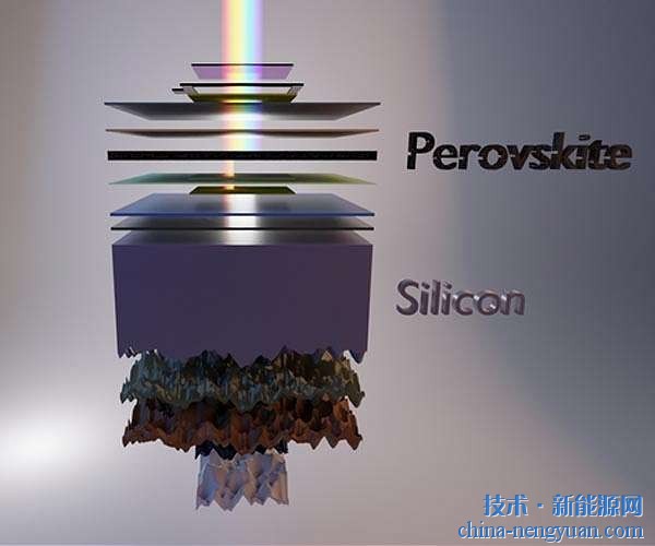
According to the report of the American Physicists Organization Network on November 9, US scientists have developed a new technology that successfully integrated composite semiconductor nanowires on silicon wafers for the first time, and met the challenges encountered in manufacturing solar cells using such semiconductors. The key challenge of lattice misalignment. They said that these tiny nanowires are expected to bring high quality, high efficiency and cheap solar cells and other electronic devices. Related research was published in the Nano Express newspaper.
Group III-V compound semiconductor refers to a compound semiconductor formed by combining group III and group V elements in an elemental periodic table, and mainly includes arsenic telluride, indium phosphide, and gallium nitride, and the electron mobility thereof is far greater than the electron mobility of silicon. Therefore, the application on high-speed digital integrated circuits is superior to that of silicon semiconductors and is expected to be used to develop devices that convert light into electricity or vice versa, such as high-end solar cells or lasers. However, they do not integrate seamlessly with the most common pedestal silicon of solar cells, thus limiting their application.
Each type of crystal material has a specific atomic distance—lattice constant (lattice constant). The biggest challenge that III-V semiconductors have encountered in the manufacture of solar cells has been that such semiconductors do not have the same crystal lattice as silicon. Constants, they can not stack together neatly stacked. The leader of the study, Li Xiuling, a professor of electronics and computer engineering at the University of Illinois, explained that when crystal lattices are not aligned, there will be misalignment between materials. Previously, scientists generally deposited Group III-V semiconductors on top of a silicon wafer covered with a thin film, but the lattice mismatch creates stress that can cause defects and degrade the performance of the resulting device.
In the latest research, the scientists abandoned the thin film and allowed a nanowire array consisting of a small, closely spaced III-V compound semiconductor to grow vertically on a silicon wafer. Li Xiuling said: "This type of nanowire geometries are better able to get rid of the limitations of lattice matching by making the mismatch strain energy disappear through the sidewalls."
The scientists discovered the different environments required for the growth of III-V semiconductors composed of different indium, arsenic, and antimony. The advantage of the latest method is that they can use ordinary growth techniques without special methods to grow nanowires on silicon wafers, nor do they need to use metal catalysts.
This nanowire geometry can enhance solar cell performance by providing higher light absorption efficiency and carrier collection efficiency, and it also uses less material than the thin film method, thus reducing costs.
Li Xiuling believes that this nanowire method can also be widely used in other semiconductors, making it possible for other applications that are hindered by lattice mismatch. His team will soon demonstrate high-quality, nanowire-based multi-junction tandem solar cells.
Cabinet Locks Co., Ltd. , http://www.nspadlocks.com